工藤
一浩 Kazuhiro Kudo
Last updated : June
30, 2016
 Kazuhiro Kudo, Professor
Graduate School of
Engineering
Chiba University
1-33 Yayoi-cho, Inage-ku, Chiba,
263-8522, Japan
千葉大学 大学院工学研究科
人工システム科学専攻 電気電子系コース
物性・デバイス教育研究領域(分子機能デバイス)
E-mail: kudo at
faculty.chiba-u.jp
略歴
1977年3月 東京工業大学工学部電子工学科卒業
1979年3月 同大学大学院理工学研究科修士課程修了
1982年3月 同大学院理工学研究科(電子物理工学専攻)博士課程修了
1982年4月 松下電器産業(株)(現:パナソミック)入社
1987年2月 千葉大学工学部
助教授
1998年7月- 千葉大学工学部 教授 (大学院工学研究科 人工システム科学専攻)
1998年10月-1999年7月 ロンドン大学客員教授
2009年-2011年 千葉大学
先進科学センター長
2012年-2014年 千葉大学
高大連携企画室長
2013年- 千葉大学
高大連携・地域貢献部門長
2015年- 千葉大学
次世代才能支援室長
所属学会:応用物理学会(フェロー)、電気学会、電子情報通信学会(フェロー)、
高分子学会
主な研究分野
ナノテクノロジーによる超薄膜構造の形成と局所光電子物性評価、
および、機能性有機薄膜デバイス、分子電子デバイスの研究
1)化合物半導体量子構造の形成と光・電子物性(1982-1998)
2)SiMOSプロセスと界面準位評価(1984-1994)
3)機能性有機超薄膜の作製と評価(1978-現在)
4)フレキシブル有機デバイス(1978-現在)
研究内容: Research Field
1)化合物半導体量子構造の形成と光・電子物性(1982-1998): Fabrication and Optoelectric Properties of Compound Semiconductor Quantum Structures
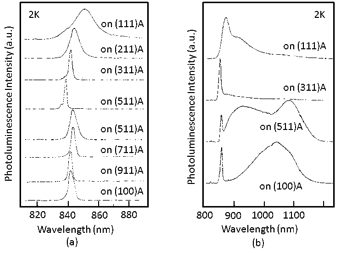
主に分子線エピタキシャル(MBE)法と有機金属化学気相成長法(MOCVD)により作製したIII-V族化合物半導体の薄膜の光・電子物性評価(フォトルミネッセンス(PL)、トラップ準位(DLTS)測定、X線回折、蛍光EXAFSなど)と種々面方位GaAs基板上に成長した量子ピラミッド構造の作製制御と半導体レーザの開発を行ってきた。
Fig. 1-A InAs quantum pyramids formed on GaAs(111)
substrate a) a few monolayers of InAs,
b) thick InAs.
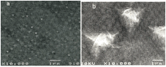
Fig. 1-B PL at 2K of (a) 1-2 monolayers InAs, (b)
InAs/GaAs SLSs (strained layer superlattices) grown
on variously oriented GaAs substrates.
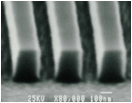
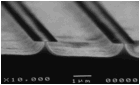
2)シリコンプロセスとMOS界面準位評価(1984-1994): Interface States and
Silicon MOS Process
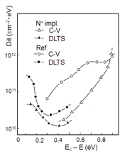
短波長光源(F2レーザ(157nm), H2放電(120-160nm), D2(115-165nm))を用いたサブミクロンリソグラフィ、ならびに、Si/SiO2界面にN+イオン注入したMOS界面準位をC-V,DLTS,TSC(熱刺激電流)法により評価を行ってきた。
Fig.
2A Submicron Lithography Fig. 2B Micro Fabrication using N+ Implantation Fig. 2C MOS Interface States measured
by C-V, DLTS
3)機能性有機超薄膜の作製と評価(1978-):Fabrication and Characterization of Functional Organic Thin
Films
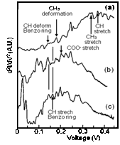
有機薄膜形成法として、真空蒸着法、ラングミュア・ブロジェット(LB)法、塗布法、印刷法による機能性薄膜を形成し、光電子物性評価を行っている。評価法として、薄膜構造評価(走査プローブ顕微鏡、電子顕微鏡、X線回折など)、光学的評価(紫外・可視・赤外域の吸収反射測定、ラマン分光など)、電気的評価(電流電圧、キャバシタンス、トンネル電流、非弾性トンネルスペクトロスコピー(IETS))、光電変換特性、熱刺激電流(TSC)などの測定を行っている。
Fig. 3A TSC of CuPc
Evaporated Films after O2,
Air Leak. Fig. 3B IETS of Adsorption LB Films. (a) CV (crystal violet), (b) MC (merocyanine),
(c) MC/CV samples.
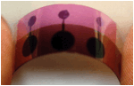
4)フレキシブル有機デバイス(1978-): Flexible Organic Devices
有機半導体薄膜を用いたフレキシブル太陽電池、トランジスタ、ディスプレイの開発研究を
行っている。新型有機トランジスタとして短チャネル化による高速・大電流縦型トランジスタ、
ドナー・アクセプタ、電荷移動錯体を用いた相転移型トランジスタ、および、フレキシブル
ディスプレイの要素素子として期待できる有機トランジスタと有機発光ダイオードを一体化
した有機発光トランジスタを開発している。
Fig.
4-A Flexible Organic
Solar Cell Fig.
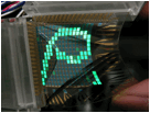
4-B Flexible OLET Display
Panel
関連論文等 (Papers)
A)Organic and Flexible
Devices(Solar Cell, Transistor, Sensor)
1) K.Kudo, S.Shiokawa, M.Yoshiura, K.Iriyama, T.Moriizumi and
T.Yasuda: Photoelectric
Effects of Thin Films Formed with Chlorophylla and/or
Chlorophyllb at Liquid/Liquid
Interfaces, Membrane, 5(2), 121123(1980)
2) K.Iriyama, M.Shiraki, K.Tsuda,
A.Okada, M.Sugi, S.Iizuma, K.Kudo, S.Shiokawa, T.Moriizumi
and T.Yasuda: Photoelectric Effects in Organic Diodes, Jpn. J. Appl. Phys.,192,
173177 (1980)
3) K.Kudo and T.Moriizumi: Photoelectric
Effects of Merocyanine ZnO Cells,
Jpn. J. Appl. Phys., 19(11), L683685(1981)
4) T.Moriizumi and K.Kudo:
MerocyanineDye Photovoltaic Cell on a Plastic Films,
Appl. Phys. Lett., 38(2), 8586(1981)
5) K.Kudo, T.Shinohara, T.Moriizumi, K.Iriyama,
M.Sugi: Study of Photovoltaic Cells
Using MerocyanineDye Thin Films, Jpn. J. Appl. Phys., 202, 135139(1981)
6) 工藤一浩, 塩川祥子, 森泉豊栄, 入山啓治, 杉
道夫: メロシアニン系色素膜の
光電変換特性, 電気学会論文誌, 101-A, 347354(1981)
7) K.Kudo and T.Moriizumi: Photoelectric
pn Junction Cells Using Organic Dyes,
Jpn. J. Appl. Phys., 20(7), L553556(1981)
8) K.Kudo and T.Moriizumi:
SpectrumControllable Color Sensors Using Organic Dyes,
Appl. Phys. Lett., 39(8), 609611(1981)
9) 工藤一浩, 篠原俊朗, 森泉豊栄: 有機色素薄膜の湿度・ガス応答特性と発・脱色現象,
電気学会論文誌, 103-A, 577583(1983)
10) K.Kudo, M.Yamashina and T.Moriizumi:
Field Effect Measurement of Organic Dye Films,
Jpn. J. Appl. Phys., 23(1), 130(1984)
11) 工藤一浩, 森泉豊栄: 分子素子, 電子情報通信学会誌,75(3), 10581064(1992)
12) K.Kudo, T.Saraya, S.Kuniyoshi and
K.Tanaka : Electrical Characterization of C60
Evaporated Films Using MOS Structure, Mol. Cryst. Liq. Cryst., 267, 423428(1995)
13) T.Sumimoto, Y.Shiratori, M.Iizuka,
S.Kuniyoshi, K.Kudo and K.Tanaka: Fabirication
and Characterization of Field Effect Transistor of Layered Structure
Consisting of
TMTSF and TCNQ, Synthetic Metals, 86, 22592260(1997)
14) M.Iizuka, S.Muraguchi, S.Kuniyoshi,
K.Kudo and K.Tanaka: Optical and Electrical Properties
of MultiLayered Organic Cells, Mol.Cryst.Liq.Cryst.,
295,5558(1997)
15) M.Iizuka, Y.Shiratori, S.Kuniyoshi,
K.Kudo and K.Tanaka: Fabrication and Characterization of
Field Effect Transistors
Using Donor and Acceptor Stacked Layers, Applied Surface Science,
130132, 914918(1998)
16) K.Kaneto, K.Kudo, Y.Ohmori, M.Onoda and
M.Iwamoto: Recent Progress in Organic Film
Devices for Optics and Electronics, IEICE Trans. Electron.,
E81C,7, 10091019 (1998)
17) K.Kudo, D.X.Wang, M.Iizuka, S.Kuniyoshi
and K.Tanaka: Organic Static Induction Transistor
for Display Devices, Synthetic Metals, 111-112, 11-14(2000)
18) H.Matsuo, S.Kuniyoshi, K.Kudo and
K.Tanaka: Evanescent Wave Fiber Optic Sensor
Using Adsorption LB Films, Synthetic Metals, 115, 37-39(2000)
19) M.Iizuka, K.Ikegami, S.Kuniyoshi, K.Kudo
and K.Tanaka: Photo-Spectral Sensitivity
Controllable Cells Using Organic Multilayer, Synthetic Metals, 115,
181-183(2000)
20) M.Iizuka, K.Kudo , S.Kuniyoshi and
K.Tanaka: Investigation of Basic Parameters in Organic
Photovoltaic Cells, Mol. Cryst. Liq. Cryst.,349, 487490(2000)
21) T.Fukagawa, M.Iizuka, S.Kuniyoshi,
K.Kudo and K.Tanaka, Growth Temperature Dependence of
the Donor-Acceptor Layered Structure FET, Mol. Cryst. Liq. Cryst., 350, 371374(2000)
22) S.Kuniyoshi, M.Iizuka, K.Kudo and
K.Tanaka: Space-Charge Conduction in a Copper
Phthalocyanine Static
Induction Transisitor, IEICE Trans. Electron., E83-C(7), 11111113(2000)
23) K.Kudo,
M.Iizuka, S.Kuniyoshi and K.Tanaka: Fabrication of New Type Field Effect
Transistors
Using Charge Transfer Complex Layers, Electrical Engineering in Japan,
134(1), 10-16(2001)
24) K.Kudo,
M.Iizuka, S.Kuniyoshi and K.Tanaka: Device Characteristics of Lateral and
Vertical
Type Organic Field Effect Transistors, Thin Solid Films, 393(1-2), 362-367(2001)
25) 工藤一浩 : 有機・高分子トランジスタ,高分子,52(2), 79-81(2002)
26) M.Iizuka, M.Nakamura and K.Kudo: Control
of FET Characteristics by Electric Field During
Charge Transfer Complex Deposition, Jpn. J. Appl.
Phys., 41(4B), 2720-2723(2002)
27) H.Sakuma, M.Iizuka, M.Nakamura, K.Kudo
and K.Tanaka: Fabrication of Field-Effect Transistor
Using
Charge-Transfer-Complex Langmuir-Blodgett Films, Jpn. J. Appl. Phys., 41,
4B, 2727-2729(2002)
28) 西村 悠,飯塚正明,中村雅一,国吉繁一,工藤一浩,田中國昭: 自己組織化スピン
コート法による有機超薄膜交互積層膜構造の作製と評価,電子情報通信学会論文誌,
J85-C12, 1057-1063(2002)
29) 田中 諭,家地洋之,飯塚正明,中村雅一,工藤一浩 : ペンタセン薄膜を用いた有機
LED駆動用トランジスタの作製,電子情報通信学会論文誌,J85-C, 12, 1083-1089(2002)
30) 工藤一浩 :アモルファスSi系に迫る有機トランジスタの開発動向,機能材料,22, 11,
47-55(2002)
31) D.Wang, M.Zhu, K.Kudo and K.Tanaka:
Study and Fabricating of Organic Semiconductor
Electroluminescence
Transistor, CHN. J. Electron., 11, 204-207(2002)
32) 中村雅一,佐久間広貴,酒井正俊,飯塚正明,工藤一浩 :「自己組織化」有機ナノ
トランジスタ,表面科学,24(2), 77-82(2003)
33) M.Nakamura, M.Fukuyo, E.Wakata,
M.Iizuka, K.Kudo and K.Tanaka: Development of AFM
Potentiometry for
Potential mapping of Organic Conductors, Synthetic Metals, 137, 887-888 (2003)
34) H.Nishimura, M.Matsuo, M.Iizuka,
S.Kuniyoshi, M.Nakamura, K.Kudo and K.Tanaka: Ultrathin
Multilayered Films Using CuPc SAS and Polyaniline, Synthetic Metals,
137, 889-890 (2003)
35) S.Kuniyoshi, M.Watanabe, M.Iizuka,
M.Nakamura, K.Kudo and K.Tanaka: Thermally Stimulated
Current of Pentacene Schottkey Diode, Synthetic Metals, 137, 895-896(2003)
36) 田中 諭,柳澤啓友,飯塚正明,中村雅一,工藤一浩 : ペンタセン蒸着膜を用いた縦型・
横型有機トランジスタ,電気学会論文誌,123, 853-857(2003)
37)
佐久間広貴,飯塚正明,中村雅一,工藤一浩 : 電荷移動錯体LB膜を用いた超薄膜
トランジスタの作製,電気学会論文誌,123, 1027-1028(2003)
38) K.Kudo, S.Tanaka,
M.Iizuka and M.Nakamura: Fabrication and Device Characterization of Organic
Light Emitting
Transistors, Thin Solid Films, 438-439, 330-333(2003)
39) M.Sakai, M.Iizuka,
M.Nakamura and K.Kudo: Fabrication and Electrical Characterization of
TTF-TCNQ Molecular
Wires, Jpn. J. Appl. Phys., 42, 2488-2491(2003)
40) 工藤一浩:有機トランジスタの現状と将来展望、応用物理,
72,1151-1156(2003)
41) K.Kudo: Optical Fiber Bio-Sensor Using
Adsorption LB Films, IEICE Trans. Electron.,
E87-C, 185-187(2004)
42) M.Sakai, M.Iizuka, M.Nakamura and K.Kudo: Thin Film Transistors
with Oriented Copper
Phthalocyanine
Crystals Fabricated by Physical Vapor Deposition under DC Electric Field,
Jpn. J. Appl. Phys.,
43, 2362-2365(2004)
43)
家地洋之、大河原 健、酒井正俊、中村雅一、工藤一浩 : 酸化亜鉛透明電極を用いた縦型
有機デバイス,電気学会論文誌C,124,
1207-1212(2004)
44) 酒井正俊、矢嶋英治、佐久間広貴、飯塚正明、中村雅一、工藤一浩 : 電荷移動錯体ワイヤ
を用いた有機ナノトランジスタ,電気学会論文誌C,124,
1224-1228(2004)
45) T.Shimada, T.Suetsugu,
T.Miyadera, Y.Yamamoto, A.Koma, K.Saiki and K.Kudo: Accelerated
Photopolymerization and
Increased Mobility in C60 Field-Effect Transistors Studied by
Ultraviolet
Photoelectron Spectroscopy, Appl. Phys. Lett., 84, 2439-2441(2004)
46) H.Sakuma, M.Sakai, M.Iizuka, M.Nakamura
and K.Kudo: Fabrication of Organic Transistors
Using BEDT-TTF and
(BEDT-TTF)(TCNQ) CT-Complex Films, IEICE Trans. Electron.,
E87-C, 12, 2049-2052(2004)
47) K.Kudo:
Organic Light Emitting Transistors, Current Applied Physics, 5, 337-340(2005)
48)
H.Nishimura, M.Iizuka, M.Sakai, M.Nakamura and K.Kudo: Poly(3-hexythiophene)
Field-Effect
Transistor with Controllable Threshold
Voltage, Jpn. J. Appl. Phys., 44, 621-625(2005)
49) M.Sakai,
E.Yajima, M.Iizuka, M.Nakamura, K.Kudo: Organic nano-transistor fabricated by
co-evaporation
method under alternating electric field, Synthetic Metals, 153,293-296 (2005)
50) H.Iechi,
M.Sakai, K.Nakamura, M.Iizuka, M.Nakamura and K.Kudo: Vertical Type Organic
Light
Emitting
Device Using Thin-film ZnO Electrode, Synthetic Metals, 154,149-152 (2005)
51)
J.M.Joseph, N.Hirashima, M.Nakamura, M.Iizuka and K.Kudo: Fabrication of
Organic Static
Induction Transistors with Higher Order Structures,
Appl. Surf. Sci., 244, 603-606(2005)
52)
Y.Watanabe and K.Kudo: Flexible Organic Static Induction Transistors Using
Pentacene Thin Films,
Appl. Phys. Lett., 87, 223505-1-3(2005)
53) 酒井正俊、中村雅一、工藤一浩:有機導体ワイヤ作製技術と有機ナノデバイスへの応用、
応用物理、75(3), 314-317(2006)
54)
Y.Watanabe, H.Iechi and K.Kudo: Improvement in On/Off Ratio of Pentacene Static
Induction
Transistors with Ultrathin CuPc Layer,
Jpn.J.Appl.Phys., 45, 3698-3703(2006)
55) H.Iechi,
Y.Watanabe and K.Kudo: Study of Vertical Type Organic Light Emitting Transistor
Using ZnO,
Proc. SPIE, Vol.6192, pp.1-7(2006)
56)
K.Nakamura, T.Hata, A.Yoshizawa, K.Obata, H.Endo and K.Kudo:
Metal-insulator-semiconductor-type
organic
light-emitting transistor on plastic substrate, Appl. Phys. Lett., 89, 103525-1-3(2006)
57)
Y.Watanabe, H.Iechi and K.Kudo: Electrical Characteristics of Flexible Organic
Static Induction
Transistors under Bending Conditions,
Appl. Phys. Lett., 89, 233509-1-3(2006)
58) N. Ohashi, M. Nakamura, N. Muraishi, M. Sakai and K.Kudo:
Fabrication and Device Simulation
of Single Nano-Scale
Organic Static Induction Transistors, IEICE Trans. Electron. E89-C(12),
1765-1770 (2006)
59) M. Xu, M. Nakamura, M. Sakai, and K. Kudo: High-Performance
Bottom-contact Organic Thin
Film Transistors with
Controlled Molecule-crystal/Electrode Interface, Adv. Mater., 19 (3),
371-375 (2007)
60) K. Fujimoto, T. Hiroi, K. Kudo, M. Nakamura: High-Performance
Vertical-Type Organic Transistor
With Built-in Nano-Triode Array, Adv. Mater.
19, 525-530(2007).
61) 岩本光正,小野田光宣,臼井博明,杉村明彦,工藤一浩: 有機界面幾何工学とエレクトロニクス,
電子情報通信学会論文誌、J90-C, 101-109(2007)
62) M.S.Xu, M.Nakamura and K.Kudo: Thickness Dependence of Mobility
of Pentacene Bottom-Contact
Organic Thin-Film Transistors, Thin Solid Films, 516,
2776-2778 (2008)
63) M.Sakai, M.Nakamura and K.Kudo: Organic Nanochannel Field-Effect
Transistor with Organic
Conductive Wires, Appl. Phys. Lett.,
90, 62101-1-3(2007)
64) H.Iechi,
M.Iizuka, Y.Watanabe and K.Kudo: Inverter Circuits Using Pentacene and ZnO
Transitors,
Jpn. J. Appl. Phys., 46, 2645-2649(2007)
65)
H.Yamauchi, M.Iizuka and K.Kudo: Fabrication of Vertical Organic Light-Emitting
Transistor
Using ZnO Thin Film, Jpn. J. Appl. Phys., 46, 2678-2682(2007)
66) Y.Watanabe, H.Iechi and K.Kudo: Improvement in On/Off Ratio
of Pentacene Static Induction
Transistors by Controlling Hole Injection
Barrier, Jpn. J. Appl. Phys., 46, 2717-2721(2007)
67) M.Xu,
K.Nagai, M.Nakamura and K.Kudo: Enhanced Performance of Solution-Processed
Regioregular Poly(3-hexylthiophene)
Thin-Film Transistors Using Planar Bottom-Contact
Architecture, Appl. Phys. Lett., 90, 223512(2007)
68) M.Sakai, H.Sakuma, Y.Ito, A.Saito, M.Nakamura and K.Kudo: Ambipolar
Field-Effect Transistor
Characteristics of (BEDT-TTF)(TCNQ) Crystals and Metal-Like
Conduction Induced by a Gate
Electric Field, Phys. Rev. B, 76, 045111-1-5(2007)
69) M.Xu,
K.Nagai, M.Nakamura and K.Kudo: Thickness
Dependence of Mobility of Pentacene Planar
Bottom-Contact Organic Thin-Film Transistors, Thin Solid Films, 516,
2776-2778 (2008)
70) 家地洋之, 渡邊康之, 山内 博, 工藤一浩: 酸化亜鉛とペンタセン薄膜トランジスタを用いた
コンプリメンタリー型論理素子の作成と評価, 電気学会論文誌, 128, 213-219 (2008)
71) M.-S. Xu,
A. Ohno, S. Aramaki, K. Kudo, M. Nakamura: Factors influencing local potential
drop
In bottom-contact organic thin-film
transistor using solution-processible tetrabenzoporphyrin,
Organic
Electronics, 9, 439-444 (2008)
72) M.Sakai,
H.Miyata, K.Itami, M.Nakamura and K.Kudo: Spontaneous Activation Process for
Self-aligned
Organic Nanochannel Transistors, Appl. Phys. Express 1, 081802-1-3(2008)
73) H. Iechi,
Y. Watanabe, H. Yamauchi and K. Kudo: Characterization of Zinc Oxide and
Pentacene
Thin Film
Transistors for CMOS Inverters, IEICE Trans. Electron., E91-C, 1843-1847(2008)
74) M.
Iizuka, H. Yamauchi and K. Kudo: Control of P3HT-FET Characteristics by
Post-Treatments,
IEICE Trans.
Electron., E91-C, 1848-1851(2008)
75) H.
Yamauchi, Y. Watanabe, M. Iizuka, M. Nakamura and K. Kudo: Characterization of
Organic
Static
Induction Transistors with Nano-Gap Gate Fabricated by Electron Beam
Lithography,
IEICE Trans.
Electron., E91-C, 1852-1855(2008)
76) H.
Yamauchi, Y. Watanabe, M. Iizuka, M. Nakamura and K. Kudo: Fabrication of
Active Light-
Emitting
Device Combined with ZnO Transistors, Jpn. J. Appl. Phys., 48,
pp.04C167-1-4(2009)
77) T. Takano, H. Yamauchi, M. Iizuka, M. Nakamura and K. Kudo:
High-Speed Operation of
Vertical Type Organic Transistors Utilizing Step-Edge Structures,
Appl. Phys. Express 2,
071501(2009)
78) H. Iechi, Y.Watanabe, H.Yamauchi, K.Kudo: Organic
Inverter Using Monolithically Stacked Static Induction Transistors, Jpn. J. Appl.
Phys., 49, 01AB12-1-4(2010)
79) 工藤一浩:有機半導体デバイスと実装技術、エレクトロニクス実装学会誌,13(2), 93-100(2010)
80) K. Kudo, T. Takano, H. Yamauchi, M. Iizuka, and M.
Nakamura: High-Speed Operation
of Step-Edge
Vertical-Channel Organic Transistors with Pentacene and 6,13-
Bis(triisopropyl-silylethynyl) Pentacene, Jpn. J. Appl. Phys.,
49, 04DK03-1-4 (2010)
81) 工藤一浩、中村雅一:縦型有機トランジスタの開発と応用展開、応用物理、79(11),
993-996(2010)
82) K.Kudo: Special Section on Recent Progress in
Molecular and Organic Devices, IEICE Trans. Electron., E94-C(2), 135(2011)
83) K. Kikuchi, F. Pu, H. Yamauchi, M. Iizuka, M. Nakamura
and K. Kudo: CMOS Circuits
Based on a
Stacked Structure Using Silicone-Resin as Dielectric Layers, IEICE Trans.
Electron.,
E94-C(2), 136-140(2011)
84) F. Pu, H. Yamauchi, H. Iechi, M. Nakamura and K. Kudo:
Organic Complementary Inverters Based on Step-Edge Vertical Channel Organic
Field-Effect Transistors, Appl. Phys. Express 4, 054203-1-3(2011)
85) M. Sakai, M. Hanada, S. Kuniyoshi, H. Yamauchi, M.
Nakamura and K. Kudo: Gate-Induced
Thermally
Stimulated Current on the Ferroelectric-like Dielectric Properties of
(BEDT-TTF)(TCNQ) Crystalline Field Effect
Transistor, Crystals, 2(3), 730-740(2012)
86) K. Kudo: Organic Electronic Devices Based on
Molecular Technology and Printing Technology,IEEJ Trans. Electron. Inform. System C, 132(9), 1392-1397(2012)
87) K. Kudo, H. Yamauchi and M. Sakai: Nanoimprinted
Step-Edge Vertical-Channel Organic Transistors, Jpn. J. Appl. Phys., 51,
11PD05-1-4 (2012)
88) K. Kudo, S. Kuniyoshi, H. Yamauchi, M. Iizuka and M. Sakai:
Vertical Channel Organic Transistors for Information Tag Applications, IEICE
Trans. Electron., E96-C(3), 340-343 (2013)
89) A. Inoue, T. Okamoto, M. Sakai, S. Kuniyoshi, H.
Yamauchi, M. Nakamura, and K. Kudo: Flexible organic field-effect transistor
fabricated by thermal press process, Physica Status Solidi A. 1-5(2013)
90) M. Sakai, T. Okamoto, Y. Yamazaki, J. Hayashi, S.
Yamaguchi, S. Kuniyoshi, H. Yamauchi, Y. Sadamitsu, M. Hamada, and K. Kudo:
Organic thin-film transistor fabricated between flexible films by thermal
lamination, Phys. Status Solidi RRL, 7,1093-1096 (2013)
91) K. Kudo, D. Tsutsumi, H. Yamauchi, S. Kuniyoshi and
M. Sakai: Vertical Channel Organic Transistors for Information Tag and Active
Matrix Display Applications, Trans. Mat. Res. Soc. Japan, 38(3), 369-372 (2013)
92) H. Yamauchi, M. Sakai, S. Kuniyoshi, K. Kudo:
Fabrication of n- and p-channel step-edge vertical-channel transistors by
electrospray deposition, Jpn. J. Appl. Phys., 53, 01AB16 (2014)
93) K. Kudo, I. Kodera, R. Aino, H. Yamauchi, S.
Kuniyoshi and M. Sakai: Fabrication of stacked logic circuits for printed
integrated circuits, Jpn. J. Appl. Phys., 05HB08 (2014)
94) A. B. Mohd Khafe, W. Sakai, H. Watanabe, H. Yamauchi,
S. Kuniyoshi, M. Sakai, K. Kudo, Ultra Violet / Ozone Thermal Treated Low
Temperature Process of Printable ZnO Field-Effect Transistor for Flexible
Displays, Jpn. J. Appl. Phys., 05FF07 (2014)
95) K. Kudo and Y. Watanabe: Organic Light-Emitting
Transistors for Flexible Active Matrix Displays, J. Imaging Soc. Japan, 53(6),
500-508 (2014) (Invited Review)
96) H. Yamauchi, S. Kuniyoshi, M. Sakai and K. Kudo:
Fabrication of Step-edge Vertical Channel Ortganic Transistors by Selective
Electrospray Deposition, IEICE Trans. Electron., E98-C, 80-85(2015)
97) R. Matsubara, Y. Sakai, T. Nomura, M. Sakai, K. Kudo,
Y. Majima, D. Knipp and M. Nakamura: Origin of mobility enhancement by chemical
treatment of gate-dielectric surface in organic thin-film transistors:
Quantitative analyses of various limiting factors in pentacene thin films, J.
Appl. Phys., 118, 175502-1-9 (2015)
98) Md. Mijanur Rahman, N. Uekawa, F. Shiba, Y. Okawa, M.
Sakai, K. Yamamoto, K. Kudo, and T. Konishi: Effect of the filtration of PbI2
solution for zinc oxide nanowire based perovskite solar cells, Jpn. J. Appl.
Phys., 55, 01AE09-1-5 (2015)
99) T. Sasaki, M. Sakai, T. Ko, Y. Okada, H. Yamauchi, K.
Kudo, Y. Sadamitsu, S. Shinamura, Solvent-free Printing of the Flexible Organic
Thin Film Transistors by Ultrasonic Welding Method, Advanced Electronic Materials,
2, 1500221-1-6 (2016)
100) H. Fukagawa, Y. Watanabe, K. Kudo, J. Nishida, Y.
Yamashita, H. Fujikake, S. Tokito and T. Yamamoto: High Current Operation of
Vertical-type Organic Transistor with Preferentially Oriented Molecular Film,
AIP Advances 6, 045010 (2016)
B)Fabrication and
Characterization of Functional Organic Films
1) C.Okazaki, S.Kuniyoshi, K.Kudo and K.Tanaka: Anodic Oxidation of Aluminum by
Electron
Tunneling Through Al/CdStearate/Al Structure, Jpn. J. Appl. Phys.,
28, L20312033(1989)
2) C.Okazaki, S.Kuniyoshi, K.Kudo and
K.Tanaka: Optical and Electrical Properties of
Selectively Adosorbed LangmuirBlodgett Films, Thin Solid Films, 179,
503507(1989)
3) C.Okazaki, S.Kuniyoshi, K.Kudo and
K.Tanaka: Molecular Interaction between Merocyanine
Dye and Several Kinds of Triphenyl Methane Derivatives in
LangmuirBlodgett Films,
Jpn. J. Appl. Phys., 29(11), 25062511(1990)
4) K.Kudo, C.Okazaki, S.Kuniyoshi and
K.Tanaka: Inelastic Electron Tunneling Spectroscopy of
LangmuirBlodgett Monolayers on Silicon Substrate, Jpn.J.Appl.Phys.,
30,7,14521456(1991)
5) S.Kuniyoshi, K.Kudo and K.Tanaka:
Infrared and Inelastic Electron Tunneling Spectroscopy of
Adsorption LangmuirBlodgett Films Containing Crystal Violet and
Merocyanine Dye,
Thin Solid Films, 210/211, 531534(1992)
6) K.Kudo, Y.Ueno, S.Kuniyoshi and T.Tanaka:
Effect of Organic Buffer Layers Using
LangmuirBlodgett Films on TCNQ Film Growth, Appl. Surf. Sci., 60/61,
334337(1992)
7) S.Kuniyoshi, K.Kudo and K.Tanaka: Doping
Effect in Merocyanine Evaporated Films,
Mol. Cryst. Liq. Cryst., 227, 199-205(1993)
8) N.Suzuki, K.Kudo, A.Taomoto, S.Kuniyoshi
and K.Tanaka: Photoelectric Effect in Single and
Double Layers of
MetalFree and Lead Phthalocyanine Evaporated Films, Mol. Cryst. Liq. Cryst.,
227, 183189(1993)
9) M.Iizuka, S.Kuniyoshi, K.Kudo and
K.Tanaka: Electrical and Optical Investigations of Carbon
Clusters Formed in Organic Films by Ion Implantation, Nucl. Instrum. Meth.,
B80/81,10721075(1993)
10) K.Kudo, H.Yageta, S.Kuniyoshi and
K.Tanaka: Surface Pressure Variation in Triphenylmethane Dye
Adsorbed Merocyanine Monolayers at the AirWater Interface, Jpn. J. Appl.
Phys., 32, 17751778(1993)
11) H.Yageta and K.Kudo: Area Variation of
Merocyanine Monolayer at the AirWater Interface
during Adsorption of Brilliant Green Dye, Jpn. J. Appl. Phys., 32, 32633264(1993)
12) 國吉繁一,近藤且章,工藤一浩,田中國昭: 「非弾性トンネルスペクトロスコピーによる
有機超薄膜の評価」 電気学会論文誌A,113,785790(1993)
13) K.Kudo, K.Itadera, S.Kuniyoshi and
K.Tanaka: Control of Molecular Adsorption by a
BiasVoltage Applied LangmuirBlodgett Technique, Thin Solid
Films, 248, 9294(1994)
14) S.Kuniyoshi, M.Nagaoka, K.Kudo,
S.Terashita, Y.Ozaki, K.Iriyama and K.Tanaka:
Inelastic Electron Tunneling Spectroscopy and Optical Characterization
of TMPD Adsorbed
CnTCNQ LangmuirBlodgett Films, IEICE TRANS.ELECTRON., E77C, 657661(1994)
15) M.Iizuka, Y.H.Yu, S.Kuniyoshi,
T.Sumimoto, K.Kudo and K.Tanaka: Fabrication and Characterization
of Modified Layer in Ion
Implanted Organic Films, Mol. Cryst. Liq. Cryst., 247, 173178(1994)
16) T.Sumimoto, S.Kuniyoshi, K.Kudo and
K.Tanaka: Effect of Several Organic Buffer Layers on
TTFTCNQ Epitaxial
Growth, Mol. Cryst. Liq. Cryst., 247, 225231(1994)
17) S.Terashita, Y.Ozaki, H.Yageta, K.Kudo
and K.Iriyama: Infrared Study of LangmuirBlodgett Films
of Chargetransfer
Complex of 2Octadecyl7,7,8,8tetracyanoquinodimethane and
Malachite
Green Prepared by Dye
Adsroption LangmuirBlodgett Technique, Langmuir, 10,18071811(1994)
18) K.Kudo, M.Nagaoka, S.Kuniyoshi and
K.Tanaka : Optical and Electrical Evaluation of
Adsorption LangmuirBlodgett Films of C18TCNQ/TMPD and C18TCNQ/PPD,
Synthetic Metals, 71, 20592060(1995)
19) T.Sumimoto, K.Kudo, T.Nagashima,
S.Kuniyoshi and K.Tanaka: Formation of TTFTCNQ
ChargeTransfer complex in Coevaporated Films, Synthetic
Metals, 70, 12511252(1995)
20) T.Sumimoto, T.Nagashima, S.Kuniyoshi,
K.Kudo and K.Tanaka : Growth of Coevaporated
TTFTCNQ Films on Surface Modified Substrates, Mol. Cryst. Liq. Cryst.,
267, 163168(1995)
21) K.Itadera, S.Kuniyoshi, M.Iizuka, K.Kudo
and K.Tanaka : Insitu Optical Monitoring of
LangmuirBlodgett Films Deposited on Optical Fibers,
Mol.Cryst.Liq.Cryst., 267, 229234(1995)
22) K.Kudo, S.Kuniyoshi and K.Tanaka : Change
of Inelastic Electron Tunneling Spectra of
Organic Ultrathin Films by Voltage Pulses and Application to
HighDensity Recording Systems,
Jpn. J. Appl. Phys.,3 4, 37823785(1995)
23) K.Itadera, S.Kuniyoshi, K.Kudo and
K.Tanaka: Fabrication of DyeAdsorbed Merocyanine Thin
Films by a Bias Voltage LangmuirBlodgett Technique, Jpn. J. Appl. Phys.,
34, 49074909(1995)
24) K.Kudo, S.Kuniyoshi and K.Tanaka: Characterization
of Molecular Films Using Inelastic
Electron Tunneling Spectroscopy and Its Application for Memory Devices,
Proc. 6th
Molecular Electronics and Devices Symposium, 8592(1995)
25) K.Yase, T.Saraya and K.Kudo: Structural
Characterization of Fullerene Thin Films Fabricated
by Organic Molecular Beam Deposition, Mat. Res. Soc. Symp. Proc., 359, 417422(1995)
26) 国吉繁一,鈴木 修, 工藤一浩, 田中國昭 : MIMおよびMIS構造における非弾性
トンネルスペクトロスコピー,電気学会論文誌,116A,8086(1996)
27) 大森 裕,岩本光正,工藤一浩: 有機超薄膜の最近の展開,電気学会論文誌,116A, 211(1996)
28) K.Itadera, K.Kako, M.Iizuka,
S.Kuniyoshi, K.Kudo and K.Tanaka : Insitu Optical Measurement of
Adsorption LB Films
Deposited on Optical Fibers, Thin Solid Films, 273, 236239(1996)
29) T.Sumimoto, M.Iizuka, S.Kuniyoshi,
K.Kudo ,K.Tanaka and Y.H.Yu: InSitu Field Effect
Measurements of Copper Phthalocyanine Films Doped with Acceptor
Molecule,
J. Korean Physical Society, 31, 522524(1997)
30) K.Kudo, T.Sumimoto, M.Iizuka, S.Kuniyoshi
and K.Tanaka: Effect of Fluorine Atoms in
Mechanically Deposited and Vapour deposited Materials on Molecular
Orientaion,
Synthetic Metals, 86, 22512252(1997)
31) K.Itadera, K.Kudo, S.Kuniyoshi and
K.Tanaka: Charge Transfer Control in Donor Molecules
Adsorbed TCNQ Thin Films by Bias Voltage LB Technique, Synthetic Metals,
86, 22612262(1997)
32) T.Sumimoto, K.Hiraga, S.Kuniyoshi,
K.Kudo and K.Tanaka: Evaluation of Electrical
Properties in P, NType Organic Thin Films by InSitu Field
Effect Measurements,
Mol. Cryst. Liq. Cryst., 294, 193196(1997)
33) K.Kudo, T.Sumimoto, K.Hiraga,
S.Kuniyoshi and K.Tanaka: Evaluation of Electrical Properties of
Evaporated Thin Films of MetalFree, Copper and Lead Phthlocyanines
by InSitu Field Effect
Measurements, Jpn. J. Appl. Phys.,36(11), 69946998(1997)
34) N.A.Kato, M.Fujimura, S.Kuniyoshi,
K.Kudo, M.Hara and K.Tanaka: Control of Molecular
Orientation of TTFTCNQ Coevaporated Films by an Applied
Electric Field, Applied Surface
Science, 130132, 658662(1998)
35) K.Hiraga, M.Iizuka, S.Kuniyoshi, K.Kudo
and K.Tanaka: Evaluation of Electrical Properties of
Merocyanine Films Doped with Acceptor or Donor Molecules by Field Effect
Measurements,
IEICE Trans. Electron., E81C,7, 10771082(1998)
36) K.Kudo, S.Kuniyoshi and Kuniaki Tanaka:
Negative Photoelectrical Properties of Adsorption
LangmuirBlodgett Films, Thin Solid Films, 327329, 399402(1998)
37) K.Itadera, K.Kudo, S.Kuniyoshi and
K.Tanaka: Fabrication and Characterization of ChargeTransfer
Complex Films by a Bias Voltage LB Technique, Thin Solid Films,
327329, 792795(1998)
38) K.Kudo, D.X.Wang, M.Iizuka, S.Kuniyoshi
and K.Tanaka: Schottky Gate Static Induction Transistor
Using Copper Phthalocyanine Films, Thin Solid Films, 331,
5154(1998)
39) 王東興,飯塚正明,国吉繁一,工藤一浩,田中國昭: 銅フタロシアニン蒸着膜を用いたショッ
トキーゲート型静電誘導トランジスタの動作特性,電気学会論文誌,118A,11661171(1998)
40) 工藤一浩,飯塚正明,国吉繁一,田中國昭 : 電荷移動錯体を用いた新型電界効果トランジ
スタの試作,電気学会論文誌,118A,14401445(1998)
41) D.X.Wang, Y.Tanaka, M.Iizuka,
S.Kuniyoshi, K.Kudo and K.Tanaka: Device Characteristics of
Organic Static Induction
Transistor Using Copper Phthalocyanine Films and Al Gate Electrode,
Jpn. J. Appl. Phys.,
38(1), 256258(1999)
42) K.Kudo, K.Shimada, K.Marugami, M.Iizuka,
S.Kuniyoshi and K.Tanaka: Organic Static Induction
Transistor for Color Sensors, Synthetic Metals, 102, 900903(1999)
43) T.Suga, M.Iizuka, S.Kuniyoshi, K.Kudo
and K.Tanaka: Determination of Effects of Purity and
Atmospheric Gases on Electrical Properties of Perylene Thin Films by
Field Effect Measurement,
Synthetic Metals, 102, 10501051(1999)
44) T.Yone, M.Iizuka, S.Kuniyoshi, K.Kudo
and K.Tanaka: Control of Molecular Orientation and
Composition Ratio of TTFTCNQ Films, Synthetic Metals, 102,
17181719(1999)
45) T.Sakabe,M.Iizuka, S.Kuniyoshi, K.Kudo
and K.Tanaka: Highly Oriented TTF-TCNQ Crystal
Growth Using Electric-Field Induced Evaporation Technique, Mol. Cryst. Liq.
Cryst., 349,
367370(2000)
46) K.Kudo, M.Iizuka, S.Kuniyoshi and
K.Tanaka: Local Area Characterization of TTF-TCNQ
Evaporated Films by Scanning Probe Microscope, IEICE
Trans.Electron.,E83-C(7),10691070(2000)
47) 飯塚正明,工藤一浩,国吉繁一,田中國昭 : イオン化蒸着法を用いた導電性分子ワイヤの
形成,電気学会論文誌,121A,628633(2001)
48)
K.Kudo: In-situ Field Effect Measurements of P-Type and N-Type Organic Thin
Films, KIEE
Trans. Elect. Appl., 12C(2), 117-122(2002)
49) M.Iizuka, N.Nakamura, K.Kudo and
K.Tanaka: Electrical Characterization of Hole Transport
Materials Using In-situ
Field Effect Measurement, IEICE Trans. Electron., E85-C(6),
131-11316(2002)
50) N.Nakamura, M.Iizuka, K.Kudo and
K.Tanaka: Local Area Characterization of Evaporated
TTF-TCNQ Complex Films
with Scanning Tunneling Spectroscopy,
IEICE Trans. Electron., E85-C(6),
13231327(2002)
51) H.Sakuma, M.Iizuka, M.Nakamura, K.Kudo:
Fabrication and characterization of ultra-thin film
transistor using TMPD-CnTCNQ LB films,
Thin Solid Films, 438-439, 326-329(2003)
52) M.Nakamura, H.Yanagisawa, S.Kuratani,
M.Iizuka, K.Kudo, K.Tanaka: Characterization of Organic
Nano-Transistors Using a
Conductive AFM Probe, Thin Solid Films, 438-439, 360-364(2003)
53) M.Nakamura, K.Kudo, A.Shimizu, Y.Nakayama and Y.Nagasawa: AFM
Study of Discrete Surface
Functional Group
Fabricated by Langmuir-Blodgett Technique, Trans. Materials Research Society
of Jpn., 28(1), 19-22(2003)
54) H.Nishimura, M.Iizuka, M.Sakai, M.Nakamura and K.Kudo:
Electrical Characterization of a P3T
Thin Film Prepared by an Applying- Field
Casting Method, Trans. Materials Research Society of
Jpn, 29,751-754(2004)
55) H.Yanagisawa,
T.Tamaki, M.Nakamura and K.Kudo: Structural and Electrical Characterization of
Pentacene Films on SiO2
Grown by Molecular Beam Deposition, Thin Solid Films, 464-465,
398-402(2004)
56) M.Sakai,
M.Iizuka, M.Nakamura and K.Kudo: Self-organized growth of tetrathiafulvalene-
tetracyanoquinodimethane molecular wires
using the co-evaporation method under a static electric
field, J. Appl. Phys.,
97,053509-1-4(2005)
57)
M.Nakamura, N.Goto, N.Ohashi, M.Sakai and K.Kudo: Potential Mapping of
Pentacene Thin-Film
Transistors Using Purely Electric
Atomic-Force-Microscope Potentiometry, Appl. Phys. Lett., 86,
122112-1-3(2005)
58)
H.Fukagawa, H.Yamane, T.Kataoka, S.Kera, M.Nakamura, K.Kudo and N.Ueno: Origin
of Highest
Occupied Band
Position in Pentacene Films from Ultraviolet Photoelectron Spectroscopy: Hole
Stabilization
versus Band Dispersion, Phys. Rev. B, 73, 245310-1-5(2006)
59)
H.Fukagawa, S.Kera, T.Kataoka, S.Hosoumi, Y.Watanabe, K.Kudo, N.Ueno: The Role
of
the
Ionization Potential in Vacumm-Level Alignment at Organic Semiconductor
Interfaces,
Adv. Mater.,
19, 665-668(2007)
60) N.Ohashi, H.Tomii, R.Matsubara, M.Sakai and K.Kudo and M.Nakamura:
Conductivity Fluctuation
within a Crystalline Domain and Its Origin in Pentacene Thin-Film
Transistors, Appl.
Phys. Lett.,
91,
162105-1-3 (2007)
61)
R.Matsubara, N.Ohashi, M.Sakai, K.Kudo and M.Nakamura: Analysis of Barrier
Height at Crystalline
Domain Boundary and In-domain Mobility in
Pentacene Polycrystalline Films on SiO2,
Appl. Phys. Lett.,
91, 242108-1-3 (2008)
62) Tomoaki
Sawabe, Koshi Okamura, Tomoki Sueyoshi, Takashi Miyamoto, Kazuhiro Kudo,
Nobuo Ueno,
Masakazu Nakamura: Vertical electrical conduction in pentacene polycrystalline
thin
films
mediated by Au-induced gap states at grain boundaries, Appl. Phys. A, 95, 225–232(2009)
63) Masakazu
Nakamura, Hirokazu Ohguri, Naoyuki Goto, Hiroshi Tomii, Mingsheng Xu, Takashi
Miyamoto,
Ryousuke Matsubara, Noboru Ohashi, Masaaki Sakai, Kazuhiro Kudo: Extrinsic
limiting
factors of carrier transport in organic field-effect transistors, Appl. Phys. A,
95, 73–80(2009)
64) 工藤一浩, 大森 裕, 岩本光正: 有機エレクトロニクスの技術進展と展望, 電子情報通信学会
論文誌C, J92-C, 488-497(2009)
65) M. Sakai, Y. Ito, T. Takahara, M. Ishiguro, M.
Nakamura and K. Kudo: Ferroelectriclike Dielectric Response and Metal-Insulator
Transition in Organic Insulator-Gate Insulator Interface, J. Appl. Phys., 107,
043711-1-5(2010)
66) M. Nakamura, A. Hoshi, M. Sakai and K. Kudo: Evaluation
of Thermopower of Organic Materials toward Flexible Thermoelectric Power
Generators, Mat. Res. Soc. Symp. Proc., 1197, 1197-D09-07 (2010)
67) N. Ohashi, H. Tomii, M. Sakai, K. Kudo, and M.
Nakamura: Anisotropy of Electrical Conductivity in a Pentacene Crystal Grain on
SiO2 Evaluated by Atomic-Force-Microscope Potentiometry and
Electrostatic Simulation, Appl. Phys. Lett., 96, 203302(3pages) (2010).
68) R. Matsubara, M. Sakai, K. Kudo, N. Yoshimoto, I.
Hirosawa and M. Nakamura: Crystal
Order in
Pentacene Thin Films Grown on SiO2 and Its Influence on Electronic Band
Structure,
Org.
Electron., 12, 195-201(2011).
69) M. Sakai, M. Iizuka, M. Nakamura and K. Kudo: Visible
effects of static electric field on physical vapor growth of lead
phthalocyanine crystals, J. Appl. Phys., 109, 054309 (7 pages) (2011).
70) K. Kudo and M. Sakai: Molecular Manipulation
Technologies Using an Electric Field and Application to Organic
Nanoelectronics, IEICE Trans. Electron., E94-C(12), 1816-1823 (2011).
71) S.-G. Li, N. Nakayama, M. Sakai, K. Kudo, R. Matsubara
and M. Nakamura: Orientational control of pentacene crystals on SiO2 by
graphoepitaxy to improve lateral carrier transport, Organic Electronics 13, 864-869(2012)
72) M. Sakai, M. Hanada, S. Kuniyoshi, H. Yamauchi, M.
Nakamura and K. Kudo: Gate-Induced Thermally Stimulated Current on the
Ferroelectric-like Dielectric Properties of (BEDT-TTF)(TCNQ) Crystalline Field
Effect Transistor, Crystals, 2(3), 730-740(2012)
73) M. Sakai, S. Kuniyoshi, H. Yamauchi, M. Iizuka, M.
Nakamura, and K. Kudo: In-situ observation of electric-field-induced
acceleration in crystal growth of tetrathiafulvalene-tetracyanoquinodimethane,
J. Appl. Phys., 113, 153513-1-6(2013)
74) F. Bussolotti, S. Kera, K. Kudo, A. Kahn and N. Ueno:
Gap states in pentacene thin film induced by inert gas exposure, Phys. Rev.
Lett., 110, 267602-1-5(2013)
75) T. Watanabe, M. Sakai, S. Unno, N. Hu, K. Kudo, H.
Ning, A. Inoue, T. Okamoto and Y. Yamazaki: Mechanical Properties of Organic
Devices Fabricated by Thermal Press Method, "Trans. Jpn. Soc. Mech. Eng.
A, 79, 1137-1141 (2013)
76) M. Sakai, Y. Yamazaki, S. Yamaguchi, J. Hayashi and
K. Kudo: Mechanical analysis of organic flexible devices by finite element
calculation, Phys. Status Solidi A, 211, 4, 795 – 799 (2014)
77) Md. Mijanur Rahman, N. Hattori, Y. Nakagawa, Xu Lin,
S. Yagai, M. Sakai, K. Kudo, and K. Yamamoto: Preparation and characterization
of silver nanoparticles on localized surface plasmon-enhanced optical
absorption, Jpn. J. Appl. Phys., 53, 11RE01-1-7 (2014)
78) M. Sakai, N. Moritoshi1, S. Kuniyoshi, H. Yamauchi,
K. Kudo and H. Masu: Partial Dissolution of Charge Order Phase Observed in
b-(BEDT-TTF)2PF6 Single Crystal Field Effect Transistor, Journal of Nanoscience
and Nanotechnology, 16, 3267–3272 (2016)
C)Fabrication and
Optoelectric Properties of Semiconductor Quantum Structures
1) Y.Makita, T.Nomura, M.Yokota,
T.Matsumori, T.Izumi, Y.Takeuchi and K.Kudo: Photoluminescence
of Very Dilutely C+ Ion Implanted GaAs, Appl. Phys. Lett.,
47(6), 623625(1985)
2) Y.Takeuchi, Y.Makita, K.Kudo, T.Nomura,
H.Tanaka, K.Irie and N.Ohnishi: Observation of New
Common Emissions in GaAs Produced by Ion Implantation of Four
Acceptor Impurities,
Appl. Phys. Lett., 48(1), 5961(1986)
3) K.Kudo, Y.Makita, I.Takayasu, T.Nomura,
T.Kobayashi, T.Izumi and T.Matsumori:
Photoluminescence Spectra of Undoped GaAs Grown by Molecular Beam
Epitaxy at Very
High and Low Substrate Temperature, J. Appl. Phys., 59(3), 888891(1986)
4) Y.Makita, T.Nomura, M.Yokota, K.Kudo and
Y.Takeuchi: Formation of Radiative ComlexCenters
by Dual Implantation of C+ and O+ Ions into GaAs,
Nucl. Instr. & Meth., B15, 765769(1986)
5) Y.Makita, K.Kudo, T.Nomura, Y.Takeuchi,
M.Yokota, Y.Mitsuhashi, T.Kobayashi, T.Izumi
and T.Matsumori: Photoluminescence of Undoped, N+ Implanted
and C+ Implanted AlAs
Grown by Molecular Beam Epitaxy, Appl. Phys. Lett.,48(24), 16871689(1986)
6) T.Nomura, Y.Makita, K.Irie, N.Ohnishi,
K.Kudo, H.Tanaka and Y.Mitsuhashi:
Concentration Ratio Dependence of Selective Optical Compensation Effect
in Dually
Zn+ and Se+ IonImplanted GaAs, Appl. Phys. Lett.,
48(25), 1745(1986)
7) Y.Makita, T.Nomura, K.Kudo, K.Irie,
N.Ohnishi, Y.Takeuchi, H.Tanaka, H.Tanoue and Y.Mitsuhashi:
Selective Optical Compensation Effect of Two New NearBandEdge
Emissions in Simultaneously
Acceptor(Zn+) and Donor(Se+) Ion Implanted GaAs, J. Appl. Phys., 60(1), 442444(1986)
8) N.Ohnishi, Y.Makita, K.Irie, K.Kudo,
T.Nomura, H.Tanaka, M.Mori and Y.Mitsuhashi:
Selective SelfOptical Compensation Effect for a Newly Discovered
AcceptorAssociated
Emission in Zn+ IonImplanted GaAs, J. Appl. Phys., 60(7),
25022504(1986)
9) K.Kudo, Y.Makita, T.Nomura, H.Tanaka,
M.Masuda and Y.Mitsuhashi: Photoluminescence of
SiDoped AlAs Grown by Molecular Beam Epitaxy, J. Appl. Phys., 60(9),
33713373(1986)
10) Y.Makiata, Y.Takeuchi, N.Ohnishi,
T.Nomura, K.Kudo, H.Tanaka, H.Lee, M.Mori and
Y.Mitsuhashi: Photoluminescence of MgDoped GaAs Grown by Molecular
Beam Epitaxy
Using Mg3As2 as a Mg Source, Appl. Phys. Lett., 49(18),
11841186(1986)
11) K.Kudo, Y.Makita, H.Oyanagi, N.Ohnishi,
T.Nomura, K.Irie, F.Uehara and Y.Mitsuhashi:
Local Structure of Heavily ZnImplanted GaAs Studied by Photoluminescence
and Fluorescence
EXAFS, Nucl. Instr. & Meth., B19/20, 398402(1987)
12) N.Ohnishi, Y.Makita, K.Kudo, T.Nomura,
H.Tanaka, K.Irie, T.Izumi, T.Kobayashi, H.Tanoue,
T.Kanayama, T.Matsumori and Y.Mitsuhashi: Photoluminescence of Strongly
Compensated GaAs
Dually Implanted by Se(Donor) and Zn(Acceptor) Ions, Nucl. Instr. &
Meth., B19/20, 403407(1987)
16)
工藤一浩: エピタキシャル層の電気・光学的評価, 精密工学会誌,56(7),3639(1990)
19) K.Kudo, J.S.Lee, K.Tanaka, Y.Makita and
A.Yamada: Fabrication and Characterization of MBE
Grown InAs/GaAs StrainedLayer Superlattices on Variously Oriented
Substrates, J. Cryst. Growth,
111, 402406(1991)
20) J.Lee, K.Kudo, S.Kuniyoshi and K.Tanaka:
Formation of InAs Microstructures on Variously
Oriented GaAs Substrate, J. Cryst. Growth, 115, 164168(1991)
21) A.Suzuki, J.Lee, K.Kudo, Y.Makita,
A.Yamada, K.Tanaka: Evaluation of Nucleation and Defects
in MBEGrown Strained InAs/GaAs Quantum Structures on Variously
Oriented Substrates,
Appl. Surf. Sci., 60/61, 631636(1992)
23) J.S.Lee, K.Kudo, Y.Makita, A.Yamada,
S.Niki and K.Tanaka: Annealing Effect in InAs/GaAs
Multiple Quantum Wells Grown on Variously Oriented Substrates, Appl. Surface
Science,
68, 251255(1993)
24) 李 定植,國吉繁一,工藤一浩,田中國昭,仁木 栄,山田昭政,牧田雄之助:複結晶配置X線
回折装置によるInAs/GaAs超薄膜の対称·非対称回折, 電気学会論文誌,113-A,741748(1993)
25) J.S.Lee, K.Kudo, S.Niki, A.Yamada,
Y.Makita and K.Tanaka: The Initial Growth Stage of the InAs
Quantum Well Structures on Variously Oriented GaAs Substrates, Jpn. J. Appl.
Phys.,
32, 48894893(1993)
26) T.Shima, J.S.Lee, K.Kudo, K.Tanaka,
S.Niki, A.Yamada and Y.Makita: Polarization Resolved
Photoluminescence of InAs/GaAs StrainedLayer Structures on
Variously Oriented Substrates,
Applied Surface Science, 75, 164168(1994)
27) J.S.Lee, T.Shima, K.Kudo, K.Tanaka,
S.Niki, A.Yamada and Y.Makita: Growth Control of InAs thin
Layers on GaAs Substrates
with Several Orientations, Applied Surface Science, 75, 279284(1994)
28) Y.Makita, T.Shima, S.Kimura, A.Obara,
K.Harada, C.W.Tu, S.Uekusa, T.Matsumori,
K.Kudo and K.Tanaka: Effect of CarbonIon IrradationEnergies on
the Molecular Beam Epitaxy of
GaAs and InGaAs, Mat. Res.
Soc. Symp. Proc., 388, 241252(1995)
29) T.Iida, K.Harada, S.Kimura, T.Shima,
H.Katsumata, Y.Makita, H.Shibata, N.Kobayashi, S.Uekusa,
T.Matsumori and K.Kudo: Heavily CarbonDoped GaAs Layers Prepared by
LowEnergy Ion
BeamImpingement during Molecular Beam Epitaxy, Nucl. Instrum. Methods,
B106, 133136(1995)
30) T.Shima, S.Kimura, T.Iida, A.Obara,
Y.Makita, K.Kudo and K.Tanaka: High Concentration Nitrogen
Ion Doping into GaAs for the Fabrication of GaAsN, Nucl. Instrum.Methods,
B118, 743747(1996)
31) T.Shima, E.Yamamoto, S.Kuniyoshi,
K.Kudo, K.Tanaka, S.Kimura, A.Obara and Y.Makita:
InPlane Photoconductivity of InAs/GaAs StrainedLayer
Structures Prepared on Variously Oriented
GaAs Substrates, Applied Surface Science, 107, 233237(1996)
32) T.Shima, Y.Makita, S.Kimura, K.Harada,
T.Iida, M.Kotani, A.Osawa, H.Shibata, A.Obara, K.Kudo,
K.Tanaka, E.Kobayashi and Y.Hoshino : Optical and Electrical
Properties of Heavily CarbonDoped
GaAs Fabricated by HighEnergy IonImplantation, Materials
Research Society Symposium
Proceedings, 396, 795800(1996)
33) T.Shima, Y.Makita, S.Kimura, T.Iida,
X.Fang, D.Jiang, K.Kudo and K.Tanaka:
Low Energy Nitrogen Ion Doping Into GaAs Using Combination Ion Beam and
Molecular
Beam Epitaxy Method, Nucl. Instrum. Methods, B120, 293297(1996)
34) T.Shima, Y.Makita, S.Kimura, T.Iida,
H.Sanpei, M.Yamaguchi, K.Kudo, K.Tanaka, N.Kobayashi,
A.Sandhu and Y.Hoshino: Optical Characterization of LowEnergy
NitrogenIon Doped GaAs,
Nucl. Instrum. Methods, B 127/128, 437441(1997)
35) A. B. Mohd Khafe, H. Watanabe, H.
Yamauchi1, S. Kuniyoshi, M. Iizuka, M. Sakai and K. Kudo:
Physical Property Evaluation of ZnO Thin Film Fabricated by
Low-Temperature Process
for Flexible Transparent TFT, J. Nanosci. Nanotech., 16, 3168–3175
(2016)
D) Interface States and Silicon MOS Process
1) S.Kuniyoshi, K.Kudo and K.Tanaka:
Electrical Conduction Properties of N+ Ion Implanted Low
Density Polyethylene Films, Proc.21 Symp. Electrical Insulating
Materials IEEE 299302(1988)
2) K.Kudo, S.Kuniyoshi and K.Tanaka: Effect
of N+ Ion Implantation on the Oxidation of
Silicon and MetalOxideSemiconductor Characteristics, Mater. Sci.
& Eng. B4, 383386(1989)
3) S.Kuniyoshi, K.Kudo and K.Tanaka: Surface
Modification of Low Density Polyethylene by
N+, Ar+ Ion Implantation for Space Charge Devices,
Appl. Sur. Sci.43, 447450(1989)
4) K.Kudo, T.Iwabuchi, K.Mutoh, T.Miyata,
R.Sano and K.Tanaka: Study of Hydrogen Vacuum
Ultraviolet Light Sources for Submicron Lithography, Jpn.J.Appl.Phys.,
29(11), 25722576(1990)
5) K.Mutoh, T.Iwabuchi, K.Kudo, H.Watanabe,
Y.Todokoro, T.Miyata and R.Sano: Nanometer
Pattern Transfer by VUV Lithography with a D2 Lamp, Jpn. J. Appl.
Phys., 29(11), 25592562(1990)
6) K.Kudo, K.Miyazaki, H.Sakai, T.Iwabuchi,
K.Mutoh, T.Miyata and T.Tomiki: Absorption
Coefficient and Sensitivity of Positive and Negative Resists in the
Vacuum Ultraviolet Region,
Jpn. J. Appl. Phys., 31(2), 401404(1992)
7) K.Kudo, S.Kuniyoshi and K.Tanaka: Dry and
Wet Etching Properties of Thermally Grown
Silicon Dioxide Layer
after N+ Ion Implantation and Annealing, Nucl. Instrum. Meth.,
B80/81, 10101013(1993)